
 by
by The global semiconductor etch equipment market is expected to double in size, reaching USD 56.1 billion by 2034, growing at a CAGR of 7.14% from 2025 to 2034, according to Precedence Research. Fueled by the miniaturization of integrated circuits and aggressive fab expansions across Asia Pacific and North America, the market is witnessing an era of transformation.
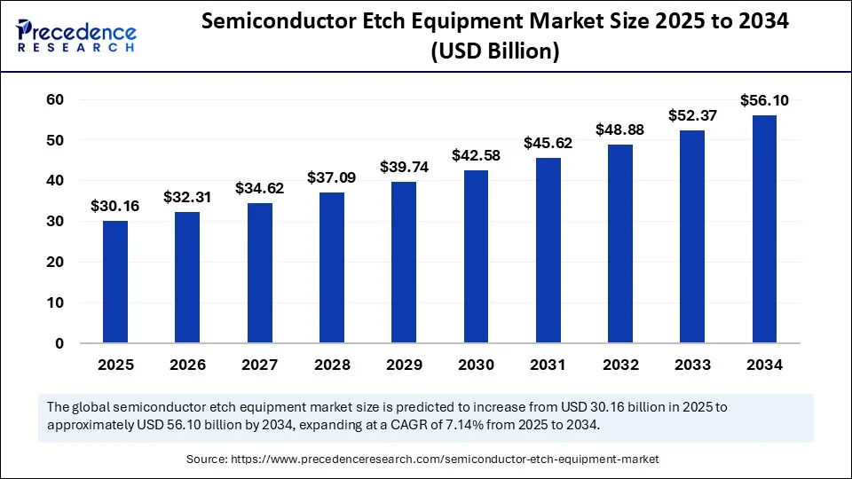
As the demand for high-performance computing, smartphones, AI, and electric vehicles continues to rise, so does the complexity of semiconductor manufacturing. A pivotal player in this chain is etch equipment, which enables precise patterning of nanostructures on silicon wafers. According to Precedence Research, the global semiconductor etch equipment market was valued at USD 28.15 billion in 2024, and is forecasted to grow at a steady CAGR of 7.14% through 2034.
The shrinking node sizes—from 10nm to 5nm and below—are driving unprecedented demand for dry and wet etch systems that can handle intricate process requirements while maintaining performance and yield.
Semiconductor Etch Equipment Market Quick Insights
-
The global market was valued at USD 28.15 billion in 2024 and is projected to reach USD 56.1 billion by 2034.
-
Asia Pacific dominated the global landscape with a 70% market share in 2024, led by foundries in Taiwan, South Korea, China, and Japan.
-
North America is a vital player with investments from Intel, GlobalFoundries, and Micron in fab capacity.
-
The dry etch equipment segment held the largest share due to its precision and compatibility with advanced nodes.
-
Key players include Lam Research, Tokyo Electron, Applied Materials, and Hitachi High-Tech.
-
The increasing use of AI and IoT devices is contributing to heightened complexity and etch demand.
Revenue Snapshot by Equipment Type
| Type | Market Share (2024) |
|---|---|
| Dry Etch Equipment | Largest Share |
| Wet Etch Equipment | Moderate Growth Expected |
How Is AI Influencing the Semiconductor Etch Equipment Market?
Artificial Intelligence is not just powering demand for advanced chips—it’s also revolutionizing the etching process itself. Through AI-powered process optimization, manufacturers can monitor plasma conditions, control etch depth, and predict wafer yield outcomes more accurately than ever before.
Moreover, AI-driven defect detection and predictive maintenance tools are significantly reducing downtime and increasing throughput. As fabs push for higher yields at lower costs, AI-integrated etching solutions are becoming indispensable.
What’s Driving the Semiconductor Etch Equipment Market Growth?
-
Demand for Smaller Nodes: As chipmakers shift to 5nm and even 3nm technologies, dry etching is indispensable due to its precision and anisotropic capabilities.
-
Expansion of Semiconductor Fabs: Aggressive fab construction plans by TSMC, Samsung, Intel, and Micron are directly boosting equipment demand.
-
Growth in AI, IoT, and EV Applications: These technologies require high-density and high-efficiency chips, elevating etching precision requirements.
-
Rise of 3D Packaging and FinFETs: These innovations need advanced etch tools that can handle complex multi-layered structures.
What Opportunities and Trends Are Emerging in the Etch Equipment Space?
Can the drive for sustainability reshape etch equipment innovation?
Yes. There’s growing demand for etching systems with low-GWP process gases, lower energy consumption, and eco-friendly chemical recycling.
Will foundry competition in Asia lead to regional fragmentation or collaboration?
While Asia Pacific remains dominant, nations are increasingly building sovereign semiconductor strategies. This is opening up cross-border collaboration for IP sharing and tech localization.
Read Also: Wide Band Gap Semiconductors Market
Semiconductor Etch Equipment Market Scope
| Report Coverage | Details |
| Market Size by 2034 | USD 56.1 Billion |
| Market Size in 2025 | USD 30.16 Billion |
| Market Size in 2024 | USD 28.15 Billion |
| Market Growth Rate from 2025 to 2034 | CAGR of 7.14% |
| Dominating Region | Asia Pacific |
| Fastest Growing Region | North America |
| Base Year | 2024 |
| Forecast Period | 2025 to 2034 |
| Segments Covered | Etching Type, Process Type, Wafer Size Compatibility, Equipment Type, Technology Node, End-Use Device Type, Application, End-User, and Region |
| Regions Covered | North America, Europe, Asia-Pacific, Latin America, and Middle East & Africa |
Expert Insight: A Consultant’s Perspective
“The race toward advanced nodes is intensifying globally. Etch equipment has moved from being just a process enabler to a strategic differentiator. We expect the next decade to witness AI-assisted, environmentally responsible etch tools redefining industry standards.”
— Rajat Malhotra, Principal Consultant – Semiconductor Equipment, Precedence Research
Semiconductor Etch Equipment Market Regional Landscape: Who’s Leading the Etch Race?
Asia Pacific:
Home to over 70% of the global market in 2024, this region is propelled by leading foundries like TSMC, Samsung, and SMIC. With government support in China and South Korea for semiconductor self-sufficiency, demand is surging across both logic and memory chip fabs.
North America:
Driven by the CHIPS and Science Act, companies such as Intel and Micron are investing billions in domestic production capabilities. The focus here is on high-end etch tools to support 3nm and 2nm nodes.
Europe:
Europe is fast catching up with its semiconductor sovereignty plans. Initiatives like the EU Chips Act are supporting fabs in Germany, France, and the Netherlands, especially for automotive-grade semiconductors.
Semiconductor Etch Equipment Market Segmental Insights
-
Etching Type:
Dry etching dominated in 2024 due to its high accuracy, ability to create complex patterns at sub-10nm nodes, and critical role in advanced chip architectures like FinFET and 3D NAND. Wet etching, while growing fast, is primarily used in packaging, MEMS, and wafer thinning thanks to its cost-effectiveness and improved precision from new chemistries. -
Process Type:
Dielectric etch led the market as it is vital for defining insulation layers in increasingly complex semiconductor devices. Growth is fueled by multi-patterning and devices demanding high-aspect-ratio structures. Meanwhile, conductor etch is on the rise, driven by shrinking interconnect pitches and the adoption of new materials for advanced logic and memory. -
Wafer Size Compatibility:
The 300mm wafers segment dominated market share in 2024 due to better cost per die and widespread adoption in large-scale fabs manufacturing logic, DRAM, and 3D NAND chips. The ≥450mm wafer segment is poised for the fastest future growth, offering further economies of scale for high-volume chip production. -
Equipment Type:
Single-wafer etch systems led in 2024, favored for their precision, process control, and adaptability to complex and multilayer chip designs. They are essential for advanced nodes and are increasingly preferred as fabs adopt high-mix, low-volume production and advanced packaging solutions. -
Technology Node:
The ≤7nm segment remained dominant, driven by the need for high-performance chips found in smartphones, SoCs, GPUs, and AI processors. Precision etching is crucial for these tiny geometries and advanced architectures such as FinFETs and GAA FETs. -
End-Use Device Type:
Logic ICs took the largest share in 2024 because CPUs, GPUs, and SoCs underpin a broad range of high-value applications. These components require ongoing process innovation and sophisticated etching, maintaining high demand for premium equipment. Memory ICs are expected to grow quickly as cloud, AI, and mobile storage needs escalate. -
Application:
The Front End of Line (FEOL) segment led in 2024, since FEOL processes—transistor patterning and gate stack formation—are critical to device reliability and performance, demanding advanced etch solutions. Packaging etch will expand rapidly as chiplet-based and 3D package technologies proliferate. -
End-User / Fabrication Facility Type:
Foundries held the largest market share because they invest heavily in advanced tools to serve diverse end-user needs across AI, mobile, automotive, and HPC sectors. OSATs (Outsourced Semiconductor Assembly and Test) are seeing rapid growth with increased adoption of advanced packaging that requires precise etching.
Company Breakthroughs & Innovations
Key players are making strategic moves to secure dominance:
-
Lam Research: Investing in AI-powered etch systems and plasma process R&D.
-
Tokyo Electron: Expanding their footprint in India and Southeast Asia.
-
Applied Materials: Collaborating with chipmakers for 3nm and 2nm readiness.
-
Hitachi High-Tech: Introducing energy-efficient etching systems.
What Are the Challenges Facing the Semiconductor Etch Equipment Market ?
-
High Capital Cost: Semiconductor etch systems are some of the most expensive tools in a fab.
-
Technology Complexity: Advanced nodes demand extremely tight control over plasma etching variables.
-
Supply Chain Instability: Global material shortages and geopolitical risks could impact delivery timelines.
Case in Point: Taiwan’s Foundry Expansion
In 2024, TSMC ramped up its 3nm fab in Taiwan, demanding hundreds of etch systems from local and global vendors. This created a 10% year-over-year increase in dry etch equipment orders, reinforcing Taiwan’s dominance in logic chip manufacturing.
Want to Know More?
Unlock deeper insights, custom breakdowns, and growth strategies tailored for your business.
📄 Download Sample Report: https://www.precedenceresearch.com/sample/6476
📅 Schedule a 1:1 Meeting with Our Analyst: sales@precedenceresearch.com
Stay ahead of the curve in semiconductor capital equipment. Explore the full potential of the etch equipment market with Precedence Research.