
 by
by 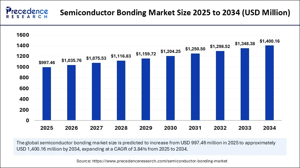
Semiconductor Bonding Market Key Insights
-
Market Size in 2024: USD 960.57 million
-
Projected Market Size by 2034: USD 1,400.16 million
-
CAGR (2025 to 2034): 3.84%
-
Dominant Region (2024): Asia Pacific (65% market share)
-
Key Companies: Panasonic Corporation, ASM Pacific Technology, Kulicke & Soffa Industries, Palomar Technologies, Hesse GmbH, Fasford Technology Co. Ltd.
-
Application Leaders: RF Devices, MEMS, CMOS Image Sensors
-
Bonding Types Covered: Die bonding, Wafer bonding
-
Top Trends: AI in chip design, 3D IC packaging, low-temperature bonding, and micro-LED display integration
👉 Download Free Sample Report https://www.precedenceresearch.com/sample/6444
What is the Role of AI in the Semiconductor Bonding Market?
AI is playing a transformative role in optimizing semiconductor bonding processes. From machine learning-driven inspection systems to AI-based predictive maintenance of bonding machines, manufacturers are streamlining throughput and yield rates like never before. AI-powered solutions are also enabling real-time defect detection and process automation, significantly reducing operational costs and enhancing chip reliability.
In advanced chip packaging, AI is used to simulate heat dissipation and optimize 3D stacking of wafers, reducing failure rates and improving device performance. As AI continues to evolve, it will deepen its integration into every phase of the bonding workflow—from alignment and placement to bonding force and time calibration.
What Factors Are Driving Market Growth?
1. Surge in Miniaturized Electronics:
The continuous push for smaller, faster, and more energy-efficient electronic devices is driving the need for precision bonding technologies. Semiconductor bonding allows manufacturers to pack more transistors into smaller footprints.
2. Rise of IoT and 5G Networks:
As IoT devices proliferate and 5G networks expand globally, chipmakers are racing to develop low-latency, high-bandwidth devices, necessitating advanced bonding for high-performance packaging.
3. Demand from Automotive & EV Industry:
Electric vehicles (EVs) and autonomous driving require a new class of power semiconductors and sensors. Semiconductor bonding ensures the ruggedness and functionality of these components in harsh conditions.
4. Growth of MEMS and CMOS Sensors:
The increasing use of MEMS in smart devices and CMOS image sensors in phones, surveillance, and automotive cameras boosts demand for wafer bonding technologies.
What Are the Emerging Opportunities and Trends in the Market?
How is technology shaping the future of semiconductor bonding?
Emerging trends such as 3D integration, wafer-to-wafer hybrid bonding, and laser-assisted bonding are reshaping semiconductor packaging. These advancements enable high-density interconnects and better thermal management, which are crucial for AI chips, VR/AR devices, and compact mobile processors.
There is also a rising demand for micro-LED displays, which require ultra-precise bonding techniques. Furthermore, low-temperature bonding methods are gaining popularity for sensitive substrates and flexible electronics. These innovations are unlocking new use cases in healthcare wearables, defense, and aerospace.
Read Also: Exosuit Materials Market
Semiconductor Bonding Market Scope
| Report Coverage | Details |
| Market Size by 2034 | USD 1,400.16 Million |
| Market Size in 2025 | USD 997.46 Million |
| Market Size in 2024 | USD 960.57 Million |
| Market Growth Rate from 2025 to 2034 | CAGR of 3.84% |
| Dominating Region | Asia Pacific |
| Fastest Growing Region | North America |
| Base Year | 2024 |
| Forecast Period | 2025 to 2034 |
| Segments Covered | Bonding Technology, Bonding Material, Packaging Type, End User, Equipment vs. Materials, and Region |
| Regions Covered | North America, Europe, Asia-Pacific, Latin America, and Middle East & Africa |
Semiconductor Bonding Market Regional Insights: Why Asia Pacific Leads the Charge
Asia Pacific dominated the global semiconductor bonding market in 2024, commanding 65% of the total revenue share, driven by the presence of large-scale semiconductor fabs and packaging houses in countries like China, Taiwan, South Korea, and Japan. These nations have become global hubs for chip assembly and test services (OSAT), thanks to strong government support and R&D investments.
North America and Europe are also significant markets, especially for automotive applications, defense-grade electronics, and advanced packaging R&D. The U.S., in particular, is witnessing renewed chip investments through the CHIPS Act.
Segmentation Analysis: End Use and Technology
The semiconductor bonding market is segmented by:
-
Type: Die Bonding, Wafer Bonding
-
Process Type: Thermocompression, Adhesive, Eutectic, Hybrid
-
Application: RF Devices, MEMS & Sensors, LED, 3D NAND, CMOS Image Sensors
-
End-Use Industry: Consumer Electronics, Automotive, Industrial, Healthcare
Among these, RF Devices and CMOS Image Sensors held a significant revenue share, while 3D NAND and MEMS are poised for rapid expansion.
Semiconductor Bonding Market Companies
- Kulicke & Soffa (K&S)
- ASM Pacific Technology (ASMPT)
- BE Semiconductor Industries (Besi)
- Shinkawa Ltd.
- Datacon
- Kulicke & Soffa’s Palomar division
- Kulicke & Soffa’s CMG division
- Nepes Corp.
- Palomar Technologies
- ThorLabs (formerly Applied Materials Assembly)
- ASM Assembly Systems
- Datacon Technology
- Europlacer
- F&K Delvotec
- SUSS MicroTec
- Tokyo Seimitsu
- Panasonic Factory Solutions
- Finetech (Kulicke & Soffa)
- Starrag Group (Jenaer)
- Intel & TSMS
Semiconductor Bonding Market Latest Breakthroughs
-
Panasonic Corporation has advanced its die bonding solutions for automotive-grade reliability.
-
ASM Pacific Technology is investing in hybrid bonding for 3D NAND flash production.
-
Kulicke & Soffa is pioneering thermocompression bonding systems for AI processors.
-
Palomar Technologies and Hesse GmbH are enhancing bonding for micro-optics and photonics applications.
These players are setting benchmarks in precision, speed, and defect-free bonding, reshaping the future of chip packaging.
Key Challenges in the Industry
Despite its potential, the semiconductor bonding industry faces challenges such as:
-
High Equipment Costs: Advanced bonding machines come with steep capital investment.
-
Thermal Stress and Defects: Misalignment or thermal mismatch during bonding can reduce chip yield.
-
Skilled Labor Shortage: Specialized knowledge is required to operate and maintain bonding equipment.
-
Supply Chain Volatility: Disruptions in semiconductor supply chains continue to impact bonding material availability.
Real-World Application: Case Study
A leading Taiwanese OSAT provider integrated AI-powered wafer bonding machines to improve throughput by 22% and reduce alignment errors by 70%. This led to a 15% cost reduction in 3D IC production, showcasing how intelligent bonding technologies are revolutionizing chip manufacturing economics.
Get the Full Report or Connect With Us
To explore more about this market schedule a consultation with our experts:
👉 You can place an order or ask any questions, please feel free to contact at sales@precedenceresearch.com |+1 804 441 9344